Troubleshooting ESP8266 FLASH connection issues
This tutorial demonstrates how to understand the interaction between the ESP8266 chip and the on-board SPI FLASH. We will create a basic “Blinking LED” application stored in the SPI FLASH and will then use the Cypress SuperSpeed Explorer kit with Analyzer2Go to capture a high-speed trace of the SPI FLASH signals, will explain how different commands in different modes are sent and how to diagnose FLASH-related problems by checking the responses to the key commands.
- Start Visual Studio and open the VisualGDB Embedded Project Wizard:
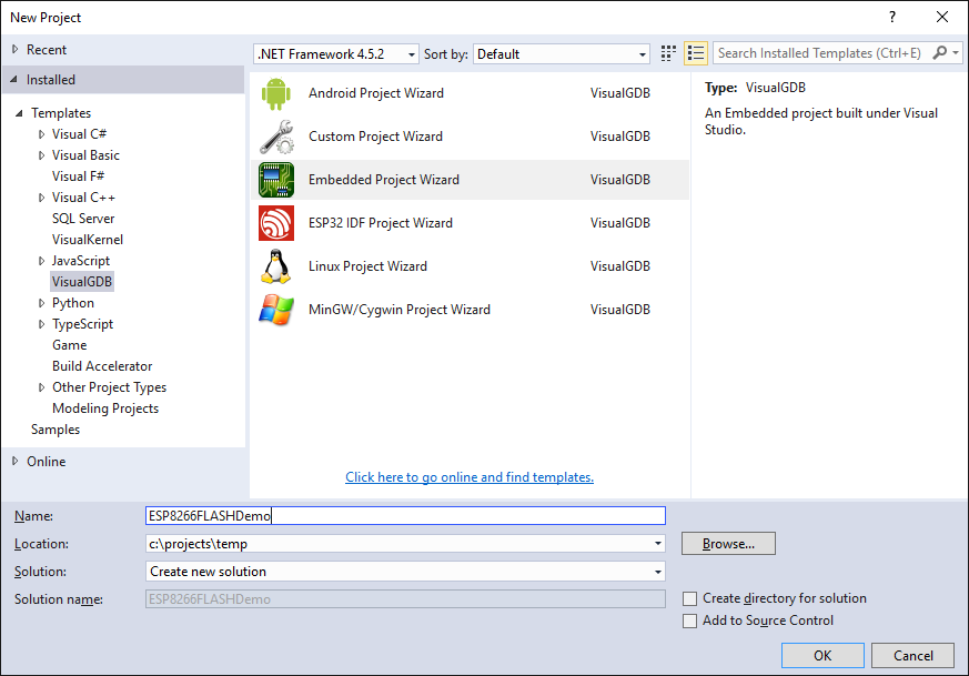
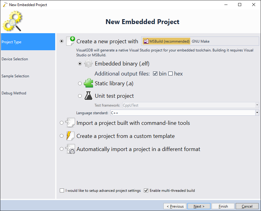
- Proceed with the default choice of creating a new project:
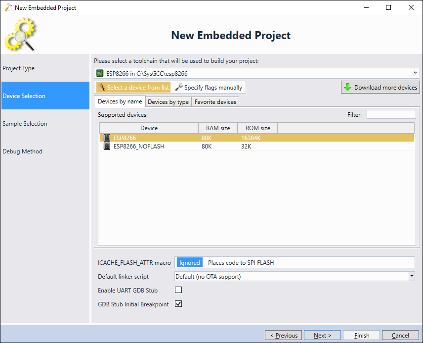
- Select the ESP8266 toolchain and proceed with the default ESP8266 device settings:
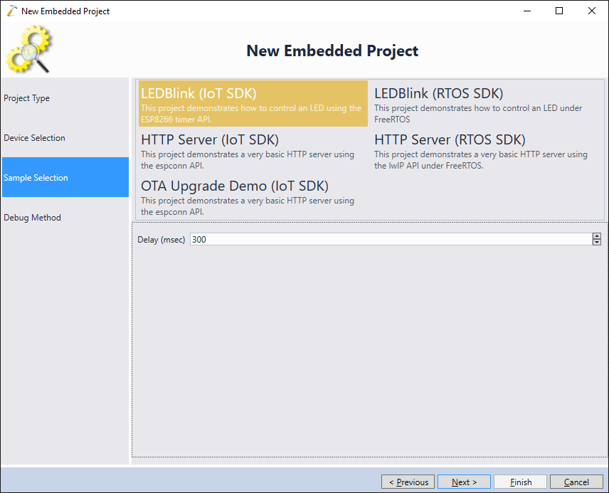
- Pick the default LEDBlink (IoT) sample and press “next”:
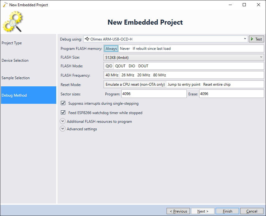
- Connect your JTAG probe via USB and pick in on the Debug Method page:
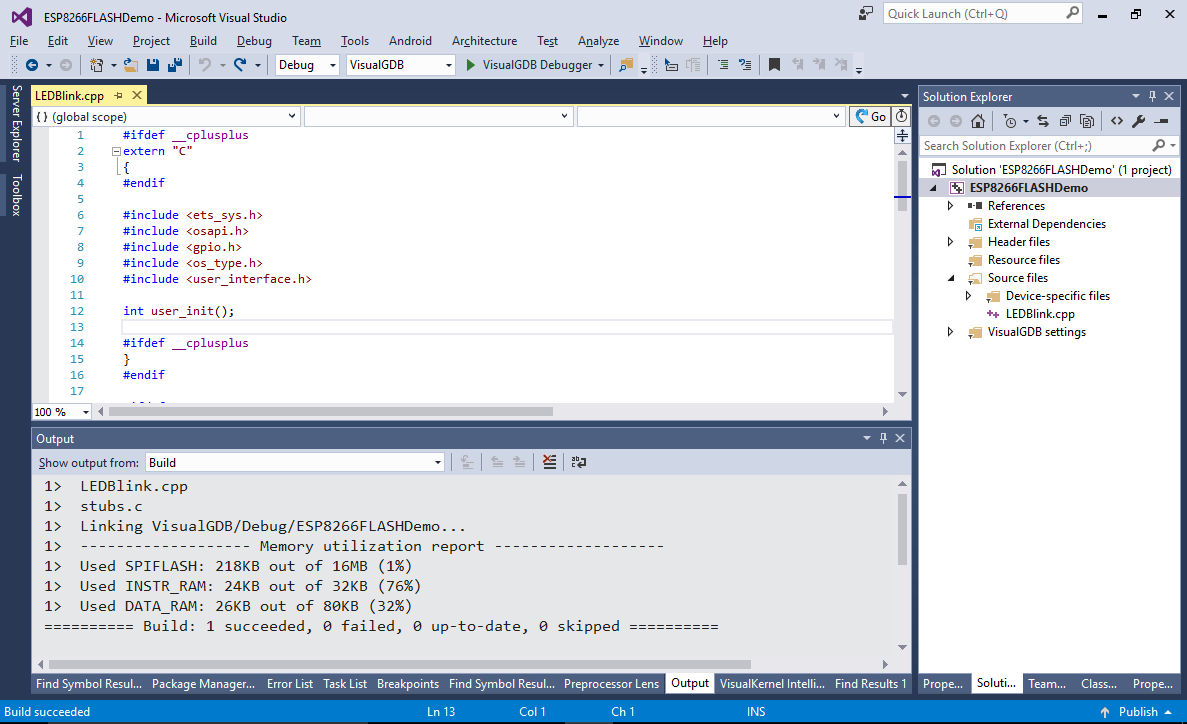
- Finally press “Finish” to create the project and build it by pressing Ctrl-Shift-B:
 Then press F5 to program the FLASH memory and begin debugging your firmware. The rest of the tutorial will show how various FLASH-related signals look like when the ESP8266 chip is accessing the FLASH memory in different modes. If your program does not run properly, compare the commands and responses captured from your board with the ones shown in this tutorial in order to pinpoint the cause.
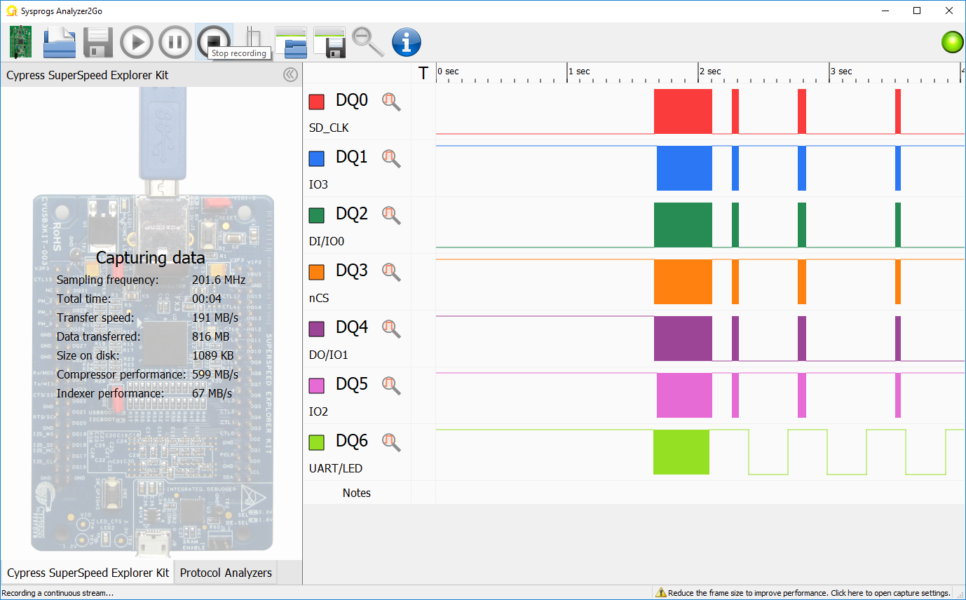
 - In order to see the interaction between the ESP8266 chip and the SPI FLASH, you will need to capture the following signals:
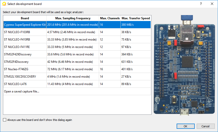
Signal Name Pin on the Olimex MOD-WIFI-ESP8266-DEV board Clock SD_CLK 5 Chip select SD_CMD 8 QSPI data pin #0 / SPI MOSI SD_DATA_0 9 QSPI data pin #1 / SPI MISO SD_DATA1 7 QSPI data pin #2 SD_DATA2 6 QSPI data pin #3 SD_DATA3 10 UART/LED output GPIO5 11 Connect them to the logic analyzer board (don’t forget to connect GND), then start Analyzer2Go and select the SuperSpeed Explorer Kit board:
 Warning! As the SPI FLASH uses relatively high frequencies, ensure that the wires connecting your logic analyzer to the ESP8266 board are as short as possible to avoid cross-talk.
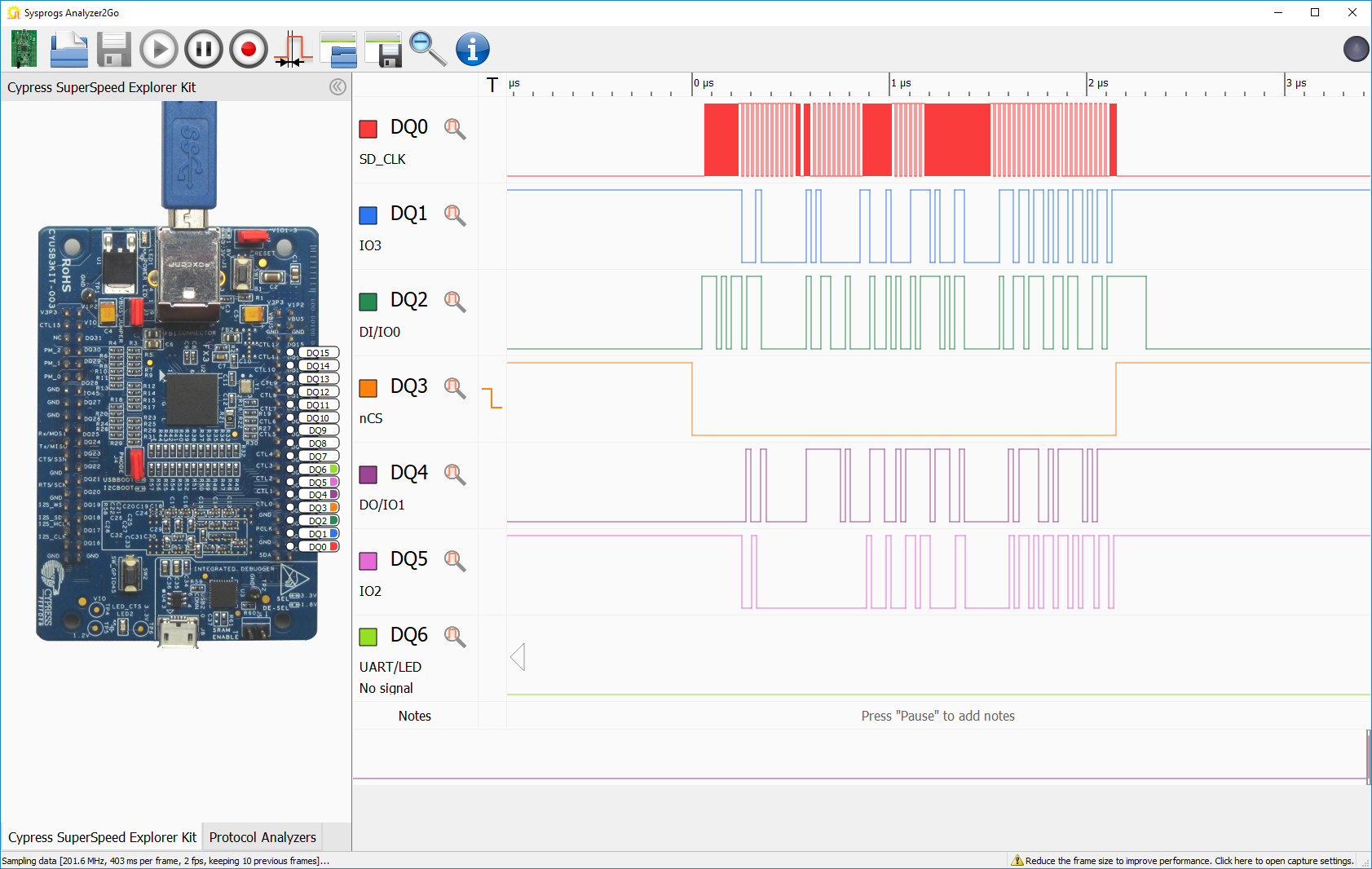
 - Press OK and enable capturing of the signals. If the firmware is running successfully, you will see short bursts of activity. During active FLASH commands the SD_CMD (nCS) pin will go low, the SD_CLK pin will start transmitting clock and the IO0-IO3 pins will be used to transfer the data:
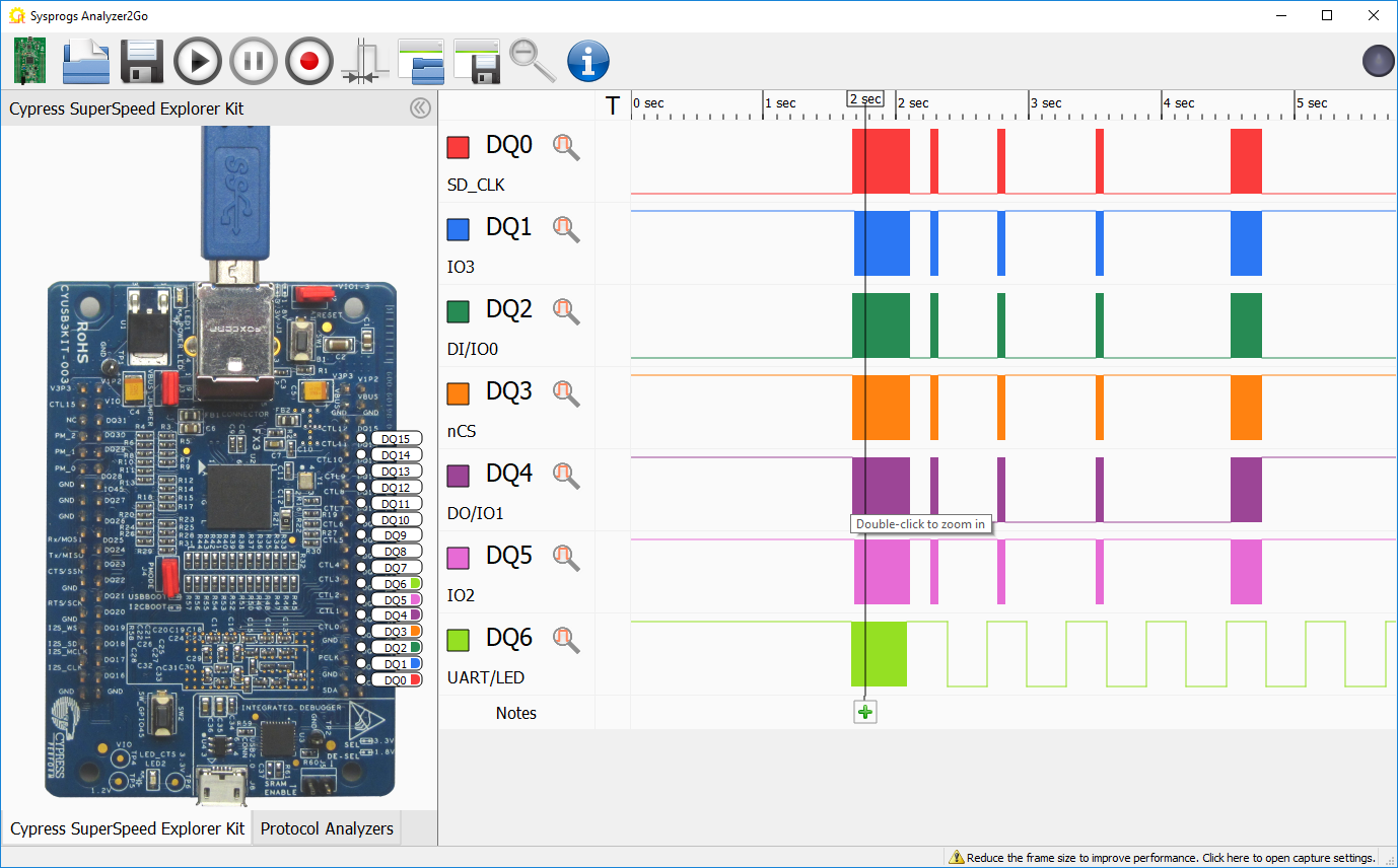
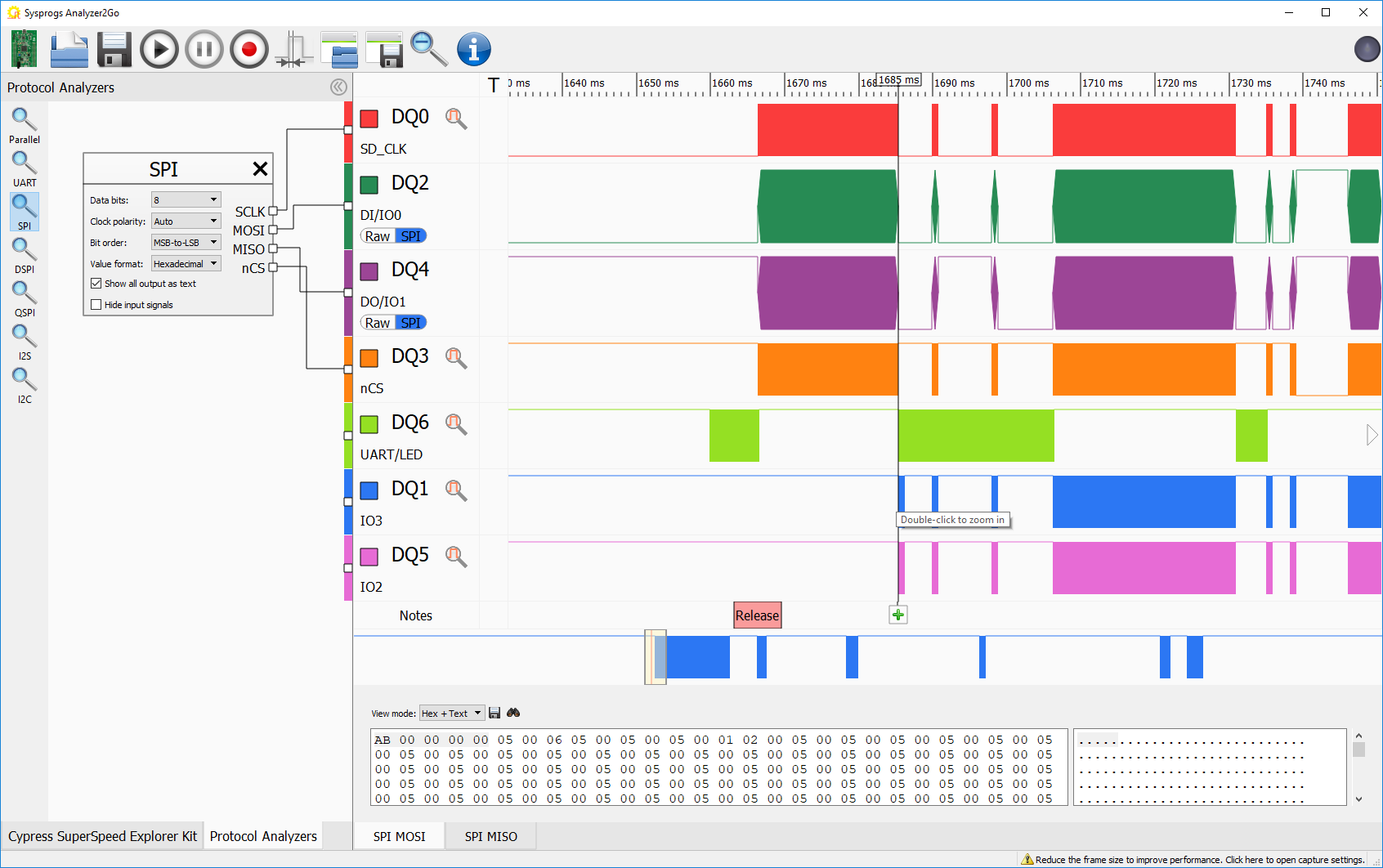
- Now we will record the entire startup sequence of the ESP8266 chip and will analyze different phases of it. Connect the Reset pin on your board to GND and press the “Record” button in Analyzer2Go. Then release the reset pin. You will see a large burst of FLASH activity followed by shorter bursts (as the LEDBlink program is very basic, most of the code will get quickly cached internally and the SPI FLASH interaction will be minimal):
- Stop recording and zoom into the first burst of SPI activity:
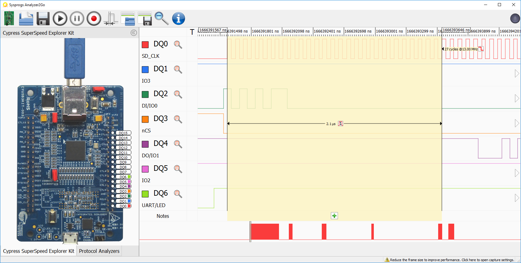
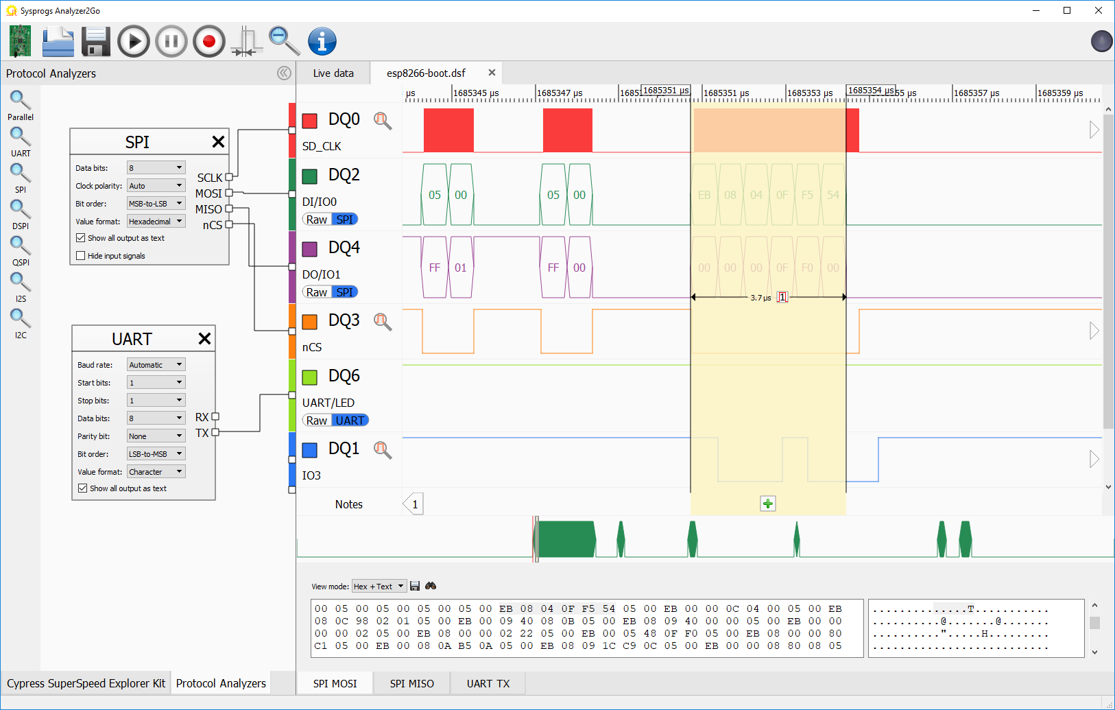
- If you zoom to the first data burst, you will see that the first SPI FLASH commands sent by the ESP8266 are using a lower 13 MHz clock, even if a higher clock rate was configured in the project properties. As the ESP8266 chip doesn’t know the FLASH type/speed at this point yet, it uses the most basic setting:
- Switch to the Protocol Analyzers tab and add the SPI analyzer. See how the first command consists of the 0xAB command byte followed by 4 zeroes and the reply from the SPI FLASH module is 0x14:
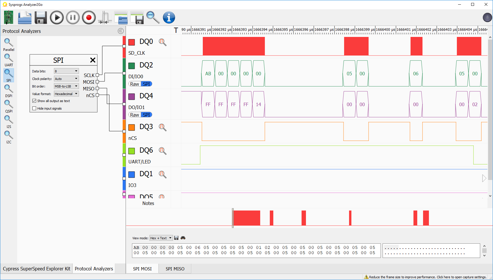
- You can find the command bytes for all commands in the QSPI FLASH datasheet. The 0xAB command releases the device from the power down mode and the device responds with its ID byte (0x14):
 Note that this command is sent using the regular SPI protocol that uses just 1 pin per direction. Most of the subsequent commands are the ESP8266 querying the status register of the FLASH module to see when it becomes ready.
 - If you zoom out of the first data burst, you will see that the QSPI pins (IO2-IO3) stay inactive during the first group of commands and become active later. Zoom in to that part of the capture:
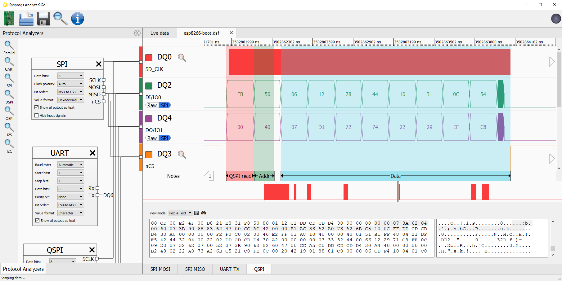
- The first command that utilizes all 4 QSPI pins is 0xEB (read data over QSPI):
- To interpret it, add a QSPI protocol analyzer to the Protocol Analyzers pane. Note that the command byte (0xEB) is transferred via the regular SPI protocol (and hence the QSPI data makes no sense for it), while the rest of the command uses the QSPI pins (hence the regular SPI data makes no sense):
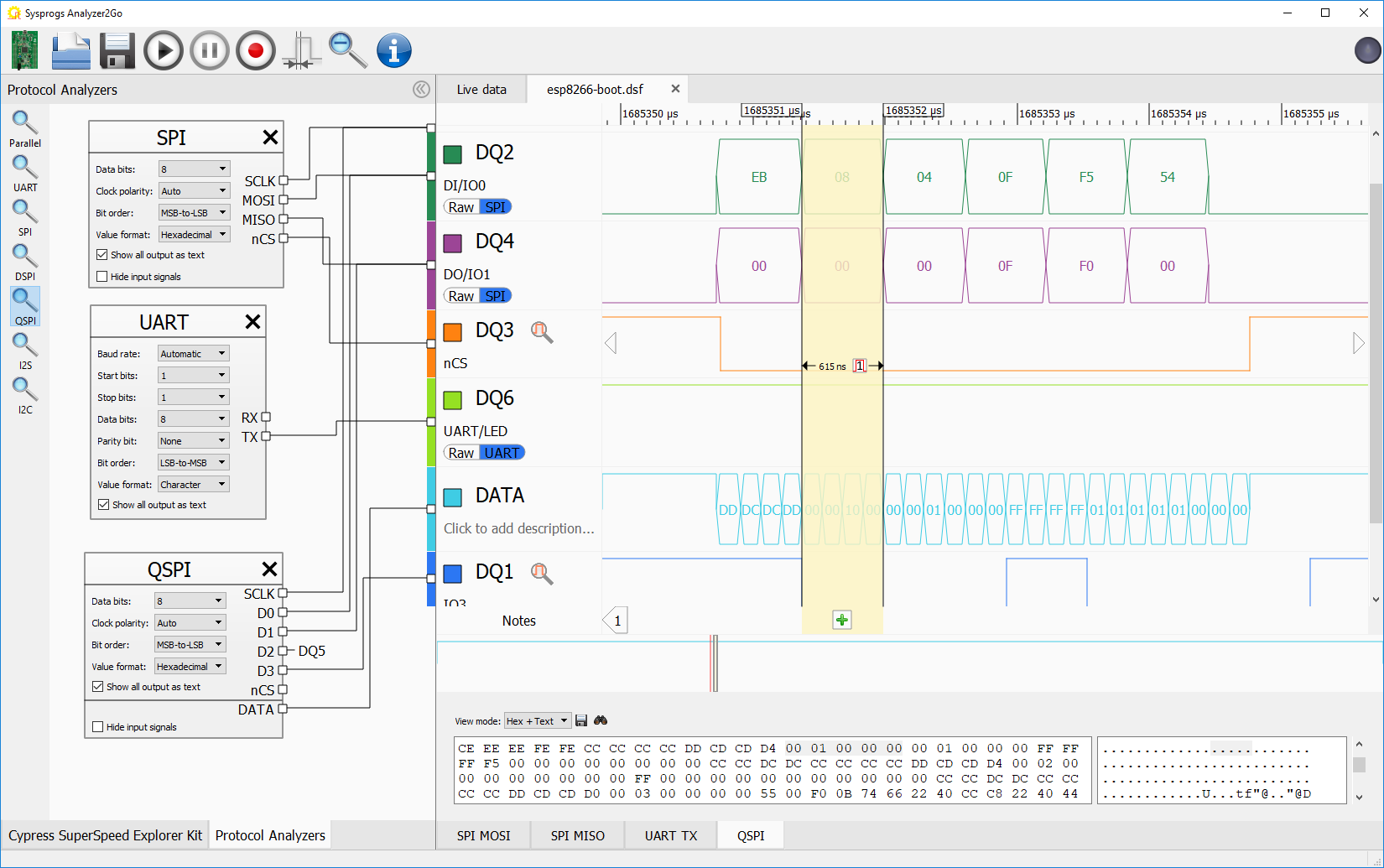
- In this example the ESP8266 reads data at address 0x00000010 and the QSPI FLASH returns the following bytes: 01 00 00 00 FF FF FF FF 01 01 01 01 01 00:
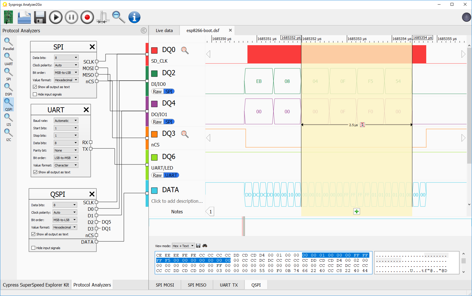
- Compare the bytes returned by the QSPI FLASH with the actual FLASH contents (either the .bin file of your project, or the FLASH snapshot created via the ESP8266 bootloader):
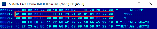
- You can use the “Show all output as text” checkbox to display all capture QSPI data in a separate pane in Analyzer2Go and search for specific patterns (e.g. read addresses):
 If the data received from the SPI FLASH doesn’t match the expected values, check that none of the SPI pins is stuck at a fixed value (0 or 1). If this is the case, double-check the connection between the ESP8266 and the SPI FLASH.
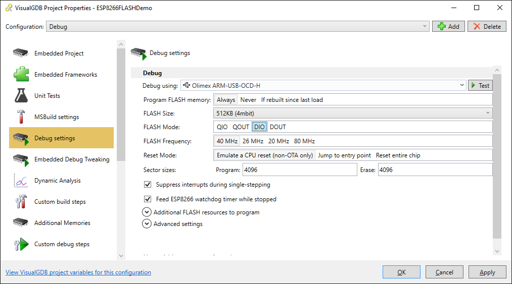
 - Now we will show how the FLASH reading commands change if you switch from QSPI to DSPI. Open VisualGDB Project Properties and switch QIO to DIO:
- Start recording with Analyzer2Go and run the firmware again. See how instead of 0xEB command, ESP8266 is now using the 0xBB command (read data via DSPI) and how the IO2 and IO3 pins are now unused:
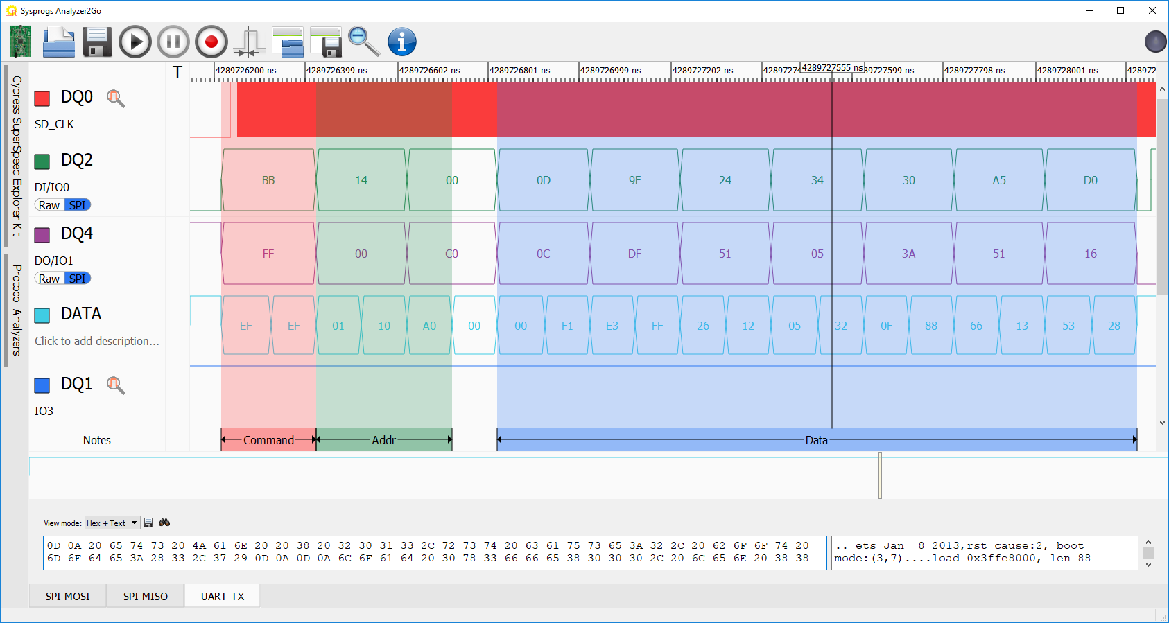
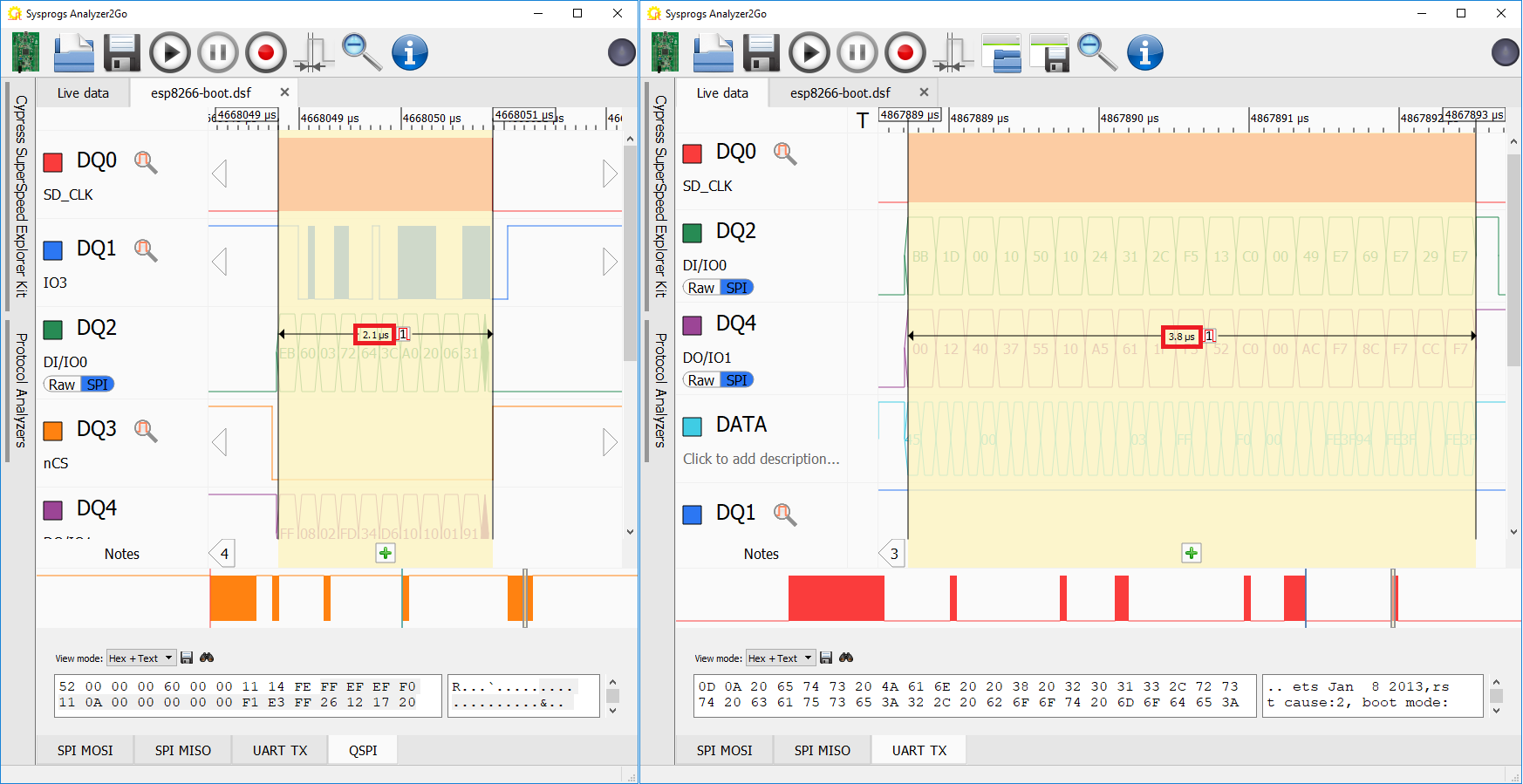
- Using DSPI instead of QSPI reduces the amount of used pins, but increases the time required to read each data chunk. You can see this by comparing the burst times in Analyzer2Go:
 You can also try experimenting with different cache settings and see how this affects the SPI FLASH reading patterns, so you can choose the right trade-off between performance and extra memory.